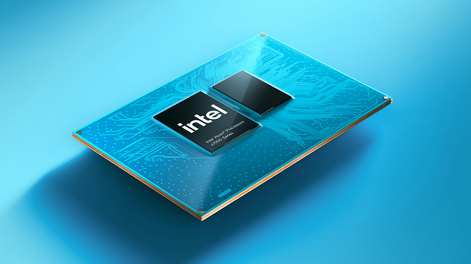
Intel has launched a new AI processor series for the edge, promising industrial-class deep learning inference. The new ‘Amston Lake’ Atom x7000RE chips offer up to double the cores and twice the higher graphics base frequency as the previous x6000RE series, all neatly packed within a 6W–12W BGA package.
The x7000RE series packs more performance into a smaller footprint. Boasting up to eight E-cores it supports LPDDR5/DDR5/DDR4 memory and up to nine PCIe 3.0 lanes, delivering robust multitasking capabilities.
Intel says its new processors are designed to withstand challenging conditions, enduring extreme temperature variations, shock, and vibration, and to operate in hard-to-reach locations. They offer 2x SATA Gen 3.2 ports, up to 4x USB 3.2 Gen 2 ports, a USB Type-C port, 2.5GbE Ethernet connection, along with Intel Wi-Fi, Bluetooth, and 5G platform capabilities.
Embedded, industrial, and communication
The x7000RE series consists of four SKUs, all suitable for embedded, industrial, and communication use under extended temperature conditions. The x7211RE and x7213RE have 2 cores and relatively lower base frequencies, while the x7433RE has 4 cores, and the x7835RE has 8 cores with higher base frequencies.
All four SKUs support a GPU execution unit count of either 16 or 32, and Intel’s Time Coordinated Computing and Time-Sensitive Networking GbE features. The x7000RE offer integrated Intel UHD Graphics, Intel DL Boost, Intel AVX2 with INT8 support, and OpenVINO toolkit support.
Intel says the chips will allow customers to easily deploy deep learning inference at the industrial edge and in smart cities, and “enhance computer vision solutions with built-in AI capabilities and ecosystem-enabled camera modules” as well as “capture power- and cost-efficient performance to enable latency-bounded workloads in robotics and automation.”
More from TechRadar Pro
Sign up to the TechRadar Pro newsletter to get all the top news, opinion, features and guidance your business needs to succeed!
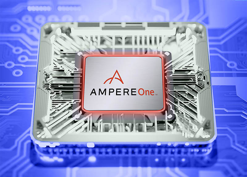
Ampere Computing unveiled its AmpereOne Family of processors last year, boasting up to 192 single-threaded Ampere cores, which was the highest in the industry.
These chips, designed for cloud efficiency and performance, were Ampere’s first product based on its new custom core leveraging internal IP, signalling a shift in the sector, according to CEO Renée James.
At the time of the launch, James said, “Every few decades of compute there has emerged a driving application or use of performance that sets a new bar of what is required of performance. The current driving uses are AI and connected everything combined with our continued use and desire for streaming media. We cannot continue to use power as a proxy for performance in the data center. At Ampere, we design our products to maximize performance at a sustainable power, so we can continue to drive the future of the industry.”
AmpereOne-3 on its way
Jeff Wittich, chief product officer at Ampere, recently spoke with The Next Platform about future generations of AmpereOne. He told the site that an updated chip, with 12 memory channels and an A2 core with improved performance, would be out later this year in keeping with the company’s roadmap. This chip, which The Next Platform calls AmpereOne-2, will reportedly have a 33 percent increase in DDR5 memory controllers and up to 50 percent more memory bandwidth.
However, what’s coming up beyond that, at some point in 2025, sounds the most exciting.
The Next Platform says the third generation chip, AmpereOne-3 as it is calling it, will have 256 cores and be “etched in 3 nanometer (3N to be precise) processes from TSMC”. It will use a modified A2+ core with a “two-chiplet design on the cores, with 128 cores per chiplet. It could be a four-chiplet design with 64 cores per chiplet.”
The site expects the AmpereOne-3 will support PCI-Express 6.0 I/O controllers and maybe have a dozen DDR5 memory controllers, although there’s some speculation here.
Sign up to the TechRadar Pro newsletter to get all the top news, opinion, features and guidance your business needs to succeed!
“We have been moving pretty fast on the on the compute side,” Wittich told the site. “This design has got about a lot of other cloud features in it – things around performance management to get the most out of all of those cores. In each of the chip releases, we are going to be making what would generally be considered generational changes in the CPU core. We are adding a lot in every single generation. So you are going to see more performance, a lot more efficiency, a lot more features like security enhancements, which all happen at the microarchitecture level. But we have done a lot to ensure that you get great performance consistency across all of the AmpereOnes. We are also taking a chiplet approach with this 256-core design, which is another step as well. Chiplets are a pretty big part of our overall strategy.”
The AmpereOne-3 is reportedly being etched at TSMC right now, prior to its launch next year.
AMD is introducing two new adaptive SoCs – Versal AI Edge Series Gen 2 for AI-driven embedded systems, and Versal Prime Series Gen 2 for classic embedded systems.
Multi-chip solutions typically come with significant overheads but single hardware architecture isn’t fully optimized for all three AI phases – preprocessing, AI inference, and postprocessing.
To tackle these challenges, AMD has developed a single-chip heterogeneous processing solution that streamlines these processes and maximizes performance.
Early days yet
The Versal AI Edge Series Gen 2 adaptive SoCs provide end-to-end acceleration for AI-driven embedded systems, which the tech giant says is built on a foundation of improved safety and security. AMD has integrated a high-performance processing system, incorporating Arm CPUs and next-generation AI Engines, with top-class programmable logic, creating a device that expertly handles all three computational phases required in embedded AI applications.
AMD says the Versal AI Edge Series Gen 2 SoCs are suitable for a wide spectrum of embedded markets, including those with high-security, high-reliability, long lifecycle, and safety-critical demands. Purposes include autonomous driving, industrial PCs, autonomous robots, edge AI boxes and ultrasound, endoscopy and 3D imaging in health care.
The processing system of the integrated CPUs includes up to 8x Arm Cortex-A78AE application processors, up to 10x Arm Cortex-R52 real-time processors, and support for USB 3.2, DisplayPort 1.4, 10G Ethernet, PCIe Gen5, and more.
The devices meet ASIL D / SIL 3 operating requirements and are compliant with a range of other safety and security standards. They reportedly offer up to three times the TOPS/watt for AI inference and up to ten times the scalar compute with powerful CPUs for postprocessing.
Sign up to the TechRadar Pro newsletter to get all the top news, opinion, features and guidance your business needs to succeed!
Salil Raje, senior vice president of AMD’s Adaptive and Embedded Computing Group, said, “The demand for AI-enabled embedded applications is exploding and driving the need for solutions that bring together multiple compute engines on a single chip for the most efficient end-to-end acceleration within the power and area constraints of embedded systems. Backed by over 40 years of adaptive computing leadership in high-security, high-reliability, long-lifecycle, and safety-critical applications, these latest generation Versal devices offer high compute efficiency and performance on a single architecture that scales from the low-end to high-end.”
Early access documentation and evaluation kits for the devices are available now. The first silicon samples of Versal Series Gen 2 are expected at the start of next year, with production slated to begin late 2025.
Samsung is reportedly planning to launch its own AI accelerator chip, the ‘Mach-1’, in a bid to challenge Nvidia‘s dominance in the AI semiconductor market.
The new chip, which will likely target edge applications with low power consumption requirements, will go into production by the end of this year and make its debut in early 2025, according to the Seoul Economic Daily.
The announcement was made during the company’s 55th regular shareholders’ meeting. Kye Hyun Kyung, CEO of Samsung Semiconductor, said the chip design had passed technological validation on FPGAs and that finalization of SoC was in progress.
Entirely new type of AGI semiconductor
The Mach-1 accelerator is designed to tackle AI inference tasks and will reportedly overcome the bottleneck issues that arise in existing AI accelerators when transferring data between the GPU and memory. This often results in slower data transmission speeds and reduced power efficiency.
The Mach-1 is reportedly a ‘lightweight’ AI chip, utilizing low-power (LP) memory instead of the costly HBM typically used in AI semiconductors.
The move is widely seen as Samsung’s attempt to regain its position as the world’s largest semiconductor company, fighting back against Nvidia which completely dominates the AI chip market and has seen its stock soar in recent months, making it the third most valuable company in the world behind Microsoft and Apple.
While the South Korean tech behemoth currently has no plans to challenge Nvidia’s H100, B100, and B200 AI powerhouses, Seoul Economic Daily reports that Samsung has established an AGI computing lab in Silicon Valley to expedite the development of AI semiconductors. Kyung stated that the specialized lab is “working to create an entirely new type of semiconductor designed to meet the processing requirements of future AGI systems.’
Sign up to the TechRadar Pro newsletter to get all the top news, opinion, features and guidance your business needs to succeed!
Now that it’s 2024, we can’t overlook the profound impact that Artificial Intelligence (AI) is having on our operations across businesses and market sectors. Government research has found that one in six UK organizations has embraced at least one AI technology within its workflows, and that number is expected to grow through to 2040.
With increasing AI and Generative AI (GenAI) adoption, the future of how we interact with the web hinges on our ability to harness the power of inference. Inference happens when a trained AI model uses real-time data to predict or complete a task, testing its ability to apply the knowledge gained during training. It’s the AI model’s moment of truth to show how well it can apply information from what it has learned. Whether you work in healthcare, ecommerce or technology, the ability to tap into AI insights and achieve true personalization will be crucial to customer engagement and future business success.
Inference: the Key to true personalisation
The key to personalisation lies in the strategic deployment of inference by scaling out inference clusters closer to the geographical location of the end user. This approach ensures that AI-driven predictions for inbound user requests are accurate and delivered with minimal delays and low latency. Businesses must embrace GenAI’s potential to unlock the ability to provide tailored and personalised user experiences.
Businesses that haven’t anticipated the importance of the inference cloud will get left behind in 2024. It is fair to say that 2023 was the year of AI experimentation, but the inference cloud will enable the realisation of actual outcomes with GenAI in 2024. Enterprises can unlock innovation in open-source Large Language Models (LLMs) and make true personalisation a reality with cloud inference.
Kevin Cochrane
Chief Marketing Officer at Vultr.
A new web app
Before the entrance of GenAI, the focus was on providing pre-existing content without personalization close to the end user. Now, as more companies undergo the GenAI transformation, we’ll see the emergence of inference at the edge – where compact LLMs can create personalized content according to users’ prompts.
Some businesses still lack a strong edge strategy – much less a GenAI edge strategy. They need to understand the importance of training centrally, inferring locally, and deploying globally. In this case, serving inference at the edge requires organizations to have a distributed Graphics Processing Unit (GPU) stack to train and fine-tune models against localized datasets.
Once these datasets are fine-tuned, the models are then deployed globally across data centers to comply with local data sovereignty and privacy regulations. Companies can provide a better, more personalized customer experience by integrating inference into their web applications by using this process.
GenAI requires GPU processing power, but GPUs are often out of reach for most companies due to high costs. When deploying GenAI, businesses should look to smaller, open-source LLMs rather than large hyperscale data centers to ensure flexibility, accuracy and cost efficiency. Companies can avoid complex and unnecessary services, a take-it-or-leave-it approach that limits customization, and vendor lock-in that makes it difficult to migrate workloads to other environments.
GenAI in 2024: Where we are and where we’re heading
The industry can expect a shift in the web application landscape by the end of 2024 with the emergence of the first applications powered by GenAI models.
Training AI models centrally allows for comprehensive learning from vast datasets. Centralized training ensures that models are well-equipped to understand complex patterns and nuances, providing a solid foundation for accurate predictions. Its true potential will be seen when these models are deployed globally, allowing businesses to tap into a diverse range of markets and user behaviors.
The crux lies in the local inference component. Inferring locally involves bringing the processing power closer to the end-user, a critical step in minimizing latency and optimising the user experience. As we witness the rise of edge computing, local inference aligns seamlessly with distributing computational tasks closer to where they are needed, ensuring real-time responses and improving efficiency.
This approach has significant implications for various industries, from e-commerce to healthcare. Consider if an e-commerce platform leveraged GenAI for personalized product recommendations. By inferring locally, the platform analyses user preferences in real-time, delivering tailored suggestions that resonate with their immediate needs. The same concept applies to healthcare applications, where local inference enhances diagnostic accuracy by providing rapid and precise insights into patient data.
This move towards local inference also addresses data privacy and compliance concerns. By processing data closer to the source, businesses can adhere to regulatory requirements while ensuring sensitive information remains within the geographical boundaries set out by data protection laws.
The Age of Inference has arrived
The journey towards the future of AI-driven web applications is marked by three strategies – central training, global deployment, and local inference. This approach not only enhances AI model capabilities but is vendor-agonistic, regardless of cloud computing platform or AI service provider. As we enter a new era of the digital age, businesses must recognize the pivotal role of inference in shaping the future of AI-driven web applications. While there’s a tendency to focus on training and deployment, bringing inference closer to the end-user is just as important. Their collective impact will offer unprecedented opportunities for innovation and personalization across diverse industries.
This article was produced as part of TechRadarPro’s Expert Insights channel where we feature the best and brightest minds in the technology industry today. The views expressed here are those of the author and are not necessarily those of TechRadarPro or Future plc. If you are interested in contributing find out more here: https://www.techradar.com/news/submit-your-story-to-techradar-pro
Large language models (LLMs) have made significant strides in artificial intelligence (AI) natural language generation. Models such as GPT-3, Megatron-Turing, Chinchilla, PaLM-2, Falcon, and Llama 2 have revolutionized the way we interact with technology. However, despite their progress, these models often struggle to provide nuanced responses that align with user preferences. This limitation has led to the exploration of new techniques to improve and customize LLMs.
Traditionally, the improvement of LLMs has been achieved through supervised fine-tuning (SFT) and reinforcement learning from human feedback (RLHF). While these methods have proven effective, they come with their own set of challenges. The complexity of training and the lack of user control over the output are among the most significant limitations.
In response to these challenges, the NVIDIA Research Team has developed a new technique known as SteerLM. This innovative approach simplifies the customization of LLMs and allows for dynamic steering of model outputs based on specified attributes. SteerLM is a part of NVIDIA NeMo and follows a four-step technique: training an attribute prediction model, annotating diverse datasets, performing attribute-conditioned SFT, and relying on the standard language modeling objective.
Customize large language models
One of the most notable features of SteerLM is its ability to adjust attributes at inference time. This feature enables developers to define preferences relevant to the application, thereby allowing for a high degree of customization. Users can specify desired attributes at inference time, making SteerLM adaptable to a wide range of use cases.
The potential applications of SteerLM are vast and varied. It can be used in gaming, education, enterprise, and accessibility, among other areas. The ability to customize LLMs to suit specific needs and preferences opens up a world of possibilities for developers and end-users alike.
In comparison to other advanced customization techniques, SteerLM simplifies the training process and makes state-of-the-art customization capabilities more accessible to developers. It uses standard techniques like SFT, requiring minimal changes to infrastructure and code. Moreover, it can achieve reasonable results with limited hyperparameter optimization.
Other articles you may find of interest on the subject of AI models
The performance of SteerLM is not just theoretical. In experiments, SteerLM 43B achieved state-of-the-art performance on the Vicuna benchmark, outperforming existing RLHF models like LLaMA 30B RLHF. This achievement is a testament to the effectiveness of SteerLM and its potential to revolutionize the field of LLMs.
The straightforward training process of SteerLM can lead to customized LLMs with accuracy on par with more complex RLHF techniques. This makes high levels of accuracy more accessible and enables easier democratization of customization among developers.
SteerLM represents a significant advancement in the field of LLMs. By simplifying the customization process and allowing for dynamic steering of model outputs, it overcomes many of the limitations of current LLMs. Its potential applications are vast, and its performance is on par with more complex techniques. As such, SteerLM is poised to play a crucial role in the future of LLMs, making them more user-friendly and adaptable to a wide range of applications.
To learn more about SteerLM and how it can be used to customise large language models during inference jump over to the official NVIDIA developer website.
Source & Image : NVIDIA
Filed Under: Technology News, Top News
Latest timeswonderful Deals
Disclosure: Some of our articles include affiliate links. If you buy something through one of these links, timeswonderful may earn an affiliate commission. Learn about our Disclosure Policy.