
[ad_1]

A few weeks ago, we wrote how Eliyan’s NuLink PHY could do away with silicon interposers and integrate everything into an single, elegant package. How, essentially, the socket could become the motherboard.
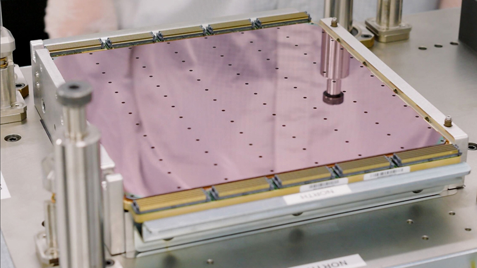
At the recent 30th annual North America Technology Symposium, the Taiwan Semiconductor Manufacturing Company (TSMC) revealed plans to construct a version of its chip-on-wafer-on-substrate (CoWoS) packaging technology that could lead to system-in-packages (SiPs) over twice the size of the current largest ones.
“With System-on-Wafer, TSMC is providing a revolutionary new option to enable a large array of dies on a 300mm wafer, offering more compute power while occupying far less data center space and boosting performance per watt by orders of magnitude,” the company said.
An enormous amount of power
TSMC’s first SoW offering, a logic-only wafer based on Integrated Fan-Out (InFO) technology, is already in production.
A chip-on-wafer version using CoWoS technology is expected to arrive in 2027, and will enable the “integration of SoIC, HBM and other components to create a powerful wafer-level system with computing power comparable to a data center server rack, or even an entire server.“
Reporting on the move, Tom’s Hardware expands on this saying, “One of the designs that TSMC envisions relies on four stacked SoICs mated with 12 HBM4 memory stacks and additional I/O dies. Such a giant will certainly draw an enormous amount of power – we are talking about thousands of watts here and will need a very sophisticated cooling technology. TSMC also expects such solutions to use a 120x120mm substrate.”
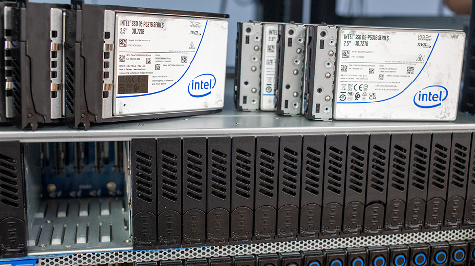
TSMC’s ambitious pursuit to create gigantic chips, however, is dwarfed by Cerebras Systems’ newest Wafer Scale Engine 3 (WSE-3), termed the “fastest AI chip in the world”. The WSE-3 boasts four trillion transistors and is twice as powerful as its predecessor, the WSE-2, while maintaining the same energy consumption and price. This new chip created on a 5nm TSMC process, provides a staggering peak AI performance of 125 petaflops – which is equivalent to 62 Nvidia H100 GPUs.
More from TechRadar Pro
[ad_2]
Source Article Link