[ad_1]
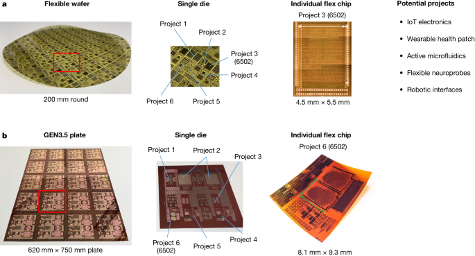
This work demonstrates the foundry model for flexible TFT technologies by designing the iconic 6502 microprocessor directly in two independent foundries—wafer-based and plate-based. The first TFT technology is based on a 200-mm round wafer approach of Pragmatic offering 0.8 µm IGZO transistors with extra metallization layers to enable higher density routing. The 6502 chip was a sub-project within the single die, as indicated in Fig. 1a. The second TFT technology is a plate-based option offering 3 µm complementary LTPS transistors. The technology of PanelSemi offers a small die of GEN-3.5 TFT panels (size 620 × 750 mm2) as base modules for the multi-project approach. Also here, Fig. 1b shows the individual 6″ die that is repeated several times across the plate, in which the 6502 is present as a sub-project. Although our recent IGZO 6502 chip has already been partially published at ISSCC22 (ref. 10), it is included in this work as a direct comparison with the 6502 plate-based chip to provide a more complete and comprehensive evaluation of foundry possibilities for flexible TFT electronics. More TFT-based companies are currently considering offering multi-project plates, such as LinkZill or Tianma, but those have not been studied in this work. Furthermore, we anticipate that more display companies and TFT foundries may adopt the presented and studied model, following the historical precedent of Si CMOS.
a, Round wafers (200 mm) offering high-density unipolar IGZO transistors. b, GEN3.5 plates offering complementary LTPS transistors. The substrate has been divided into smaller dies with individual projects. The focus of this work is on the 6502 microprocessor that has been taped out in both technologies. Panel a, image ‘Project 3 (6502)’, adapted with permission from ref. 10, IEEE.
The 6502 processor was one of the first commercial microprocessors introduced in 1975 and integrated into many products of the 1980s, such as the Nintendo Entertainment Systems, the Commodore 64 and the Apple II (ref. 25). The original version, fabricated in an 8-µm nMOS-only technology, consists of 3,510 enhancement-mode transistors and 1,018 depletion-load pull-up transistors, adding up to 4,528 devices. The microprocessor had an 8-bit data bus and 16-bit address bus, operating at 1 MHz. Owing to the legendary nature of this processor and all its ground-breaking aspects in application and microprocessor research from that time onwards, we have selected this chip to use as a vehicle to demonstrate the foundry mode with TFTs.
The logic topology for digital gates must be optimally designed according to the foundry specifications, either offering unipolar or complementary transistor technologies. These logic topologies are depicted in Supplementary Fig. 1. The most straightforward design option is a complementary inverter, which can be realized by the combination of LTPS nMOS and pMOS transistors. As classically known, this is the most robust solution, yielding the least power consumption. As TFT technologies do not always offer complementary semiconductors, many studies have been performed on inverter implementations for unipolar IGZO transistors. On the basis of these, we have opted for a pseudo-CMOS approach26,27. This requires four transistors and one extra power rail to realize an inverter. This is different from the original MOS devices in the 1970s, in which local doping profiles can yield enhancement and depletion devices. The used circuit topology at that time is also depicted in Supplementary Fig. 1, which is an interesting logic style imposing fewer transistors for complex gates, even compared with CMOS inverters, at the cost of static power consumption. A two-input NOR gate uses three transistors for the depletion-load nMOS logic style, six n-type IGZO transistors for the pseudo-CMOS implementation and four LTPS complementary transistors. IGZO or unipolar TFT technologies could also benefit from the availability of a second threshold voltage, created by technology options, such as local doping by additional treatments28,29,30 or by the introduction of a second gate26, which, after maturation can be offered through the foundry access.
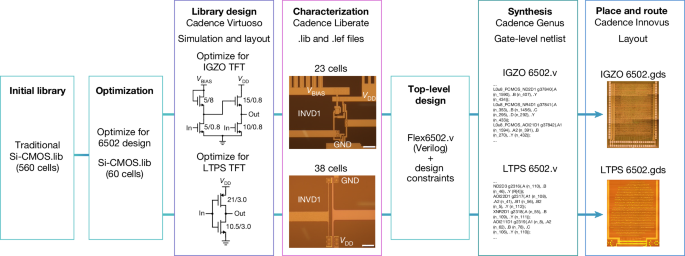
Circuit schematics of the IGZO pseudo-CMOS and LTPS CMOS inverters are shown in Fig. 3, including the selected device sizes in µm. For pseudo-CMOS logic, the input port of the inverter is connected to the gate terminals in the pull-down network to form the logic function, whereas other TFTs play the part of the pull-up network (Fig. 3). For complementary logic with LTPS technology, n-type and p-type devices with 3 µm channel length are used. The channel width ratio is selected to be 2:1 (p-TFT:n-TFT) for obtaining a symmetrical drive strength of pull-down and pull-up similar to that for Si CMOS inverters.
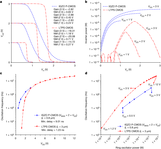
Figure 2a shows the measured d.c. characteristics of both inverter architectures for various supply voltages (VDD), ranging from 1 V to 3 V. Correct operation of a pseudo-CMOS inverter relies on the condition that the second supply voltage (VBIAS) is equal to or at least one VT larger than VDD, yielding a rail-to-rail swing of the output voltage. Moreover, increasing the VBIAS shifts the voltage transfer curve in the right direction, which can be useful for post-fabrication tuning of the static noise margin, depending on the local VT and variability values10. Figure 2a shows the voltage transfer curves in which VBIAS equals twice VDD for pseudo-CMOS logic. Figure 2b shows the logarithmic power consumption curves with respect to Vin for all logic styles, in which a difference in static power consumption of more than six orders of magnitude is observed. The static power when Vin is logic 0 stems from the leakage of n-type devices because of the VT difference in technologies.
a, Measured voltage transfer characteristics of IGZO pseudo-CMOS and LTPS CMOS inverters for various VDD supplies. b, Measured power in logarithmic scale compared with input voltage of inverters. c, Measured ring oscillator frequency compared with its supply voltage for both technologies. d. Corresponding frequency versus power plot for each technology. P-CMOS, pseudo-CMOS; Min., minimum; NM, noise margin.
To compare the performance and power consumption metrics of both inverter architectures, 19-stage ring oscillator circuits are designed and characterized (Supplementary Fig. 3). Figure 2c shows the oscillation frequency values with respect to VDD supply, in which VBIAS equals twice VDD for pseudo-CMOS. The CMOS inverter can achieve a stage delay lower than 1.5 ns when operated at large supply voltages. The oscillation frequency of those ring oscillator inverters is plotted versus the power consumption in Fig. 2d. The LTPS CMOS inverter consumes less power regardless of supply voltage because of its complementary structure.
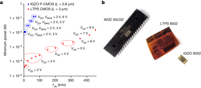
We have subsequently designed and realized 6502 chips in both available foundry technologies, according to the industry-ready design flow, starting from a traditional CMOS library with a strong focus on optimizing cells frequently used for the 6502 design. This is schematically represented in Fig. 3, and more details on the flow are explained in the Methods. Both chips have been characterized with a 48-pin probe card after the fabrication cycle, without dicing and delamination. The probe card includes level shifters to enable verification with an FPGA that generates the clock, the 64 kB memory and universal asynchronous receiver–transmitter (UART) (for more details, see the Methods). Figure 4a shows the resulting minimum power consumption that is required to reach different clock frequencies, up to 454 kHz. It is unfair and not necessary to directly compare both chips because of the absence of a complementary semiconductor in IGZO and more importantly because of the different application cases for both technologies. Nonetheless, both of them are fully functional and show predictable specifications related to their underlying transistor technology.
Lots of similarities can be observed. The main difference is the complexity of the cell library, being more complex for LTPS because of the benefits of complementary logic gates. Scale bars, 20 μm. Image ‘IGZO 6502.gds’ adapted with permission from ref. 10, IEEE.
a, The minimum power consumption of the characterized 6502 chips to reach different clock frequencies (fclk). b, Photograph of all three chips at once: the vintage WDC 65C02 in a 40-pin DIP package (left), the flex LTPS 6502 (middle) and the flex IGZO 6502 (right)10.
Table 1 summarizes the results of the 6502 microprocessor implementations for all discussed technologies—namely, the original nMOS, the n-type IGZO (ref. 10) and the newest CMOS LTPS version until now. Impressively, the original MOS6502 yields the lowest transistor count, which may differ because of an optimized version in the 1970s compared with an open-source version used for both the flex implementations. Moreover, in those early days, the only possibility to realize a design was a full-custom flow, in which the semi-custom flow nowadays is mandatory to maintain a reasonable design time while creating some overhead. Another difference is the number of transistors per logic gate, which is higher for both flex implementations. Moreover, the arithmetic and logic unit has not been optimized for the flexible 6502 versions, and traditional standard cells have been used. Table 1 also reports the characterized yield of functional 6502 implementations in both technologies. We observed a 42% yield of the Flex IGZO 6502 in Pragmatic technology with an unoptimized design for yield. We did not focus on any design for manufacturing approach to increase the yield figure as it was out of scope for our research. The yield has been determined by characterizing 104 chips across three wafers. A more thorough analysis of yield figures in Pragmatic technology as a function of chip complexity has been studied recently11. Similarly, for LTPS, we have measured 100 samples over several GEN3.5 plates and achieved a yield of 89%. A typical coloured die map can be seen in Supplementary Fig. 5. Figure 4b shows a photo of all microprocessors at once. Both chips show the key advantages of the multi-project wafer concept for both wafer-based and plate-based technologies. Supplementary Fig. 6 details the yield data specifically per frequency for 85 evaluated LTPS 6502 processors. Each processor worked at 357.1 kHz, whereas only a selection can be operated at 416.7 kHz. The lowest fraction, 23 processors, showed correct behaviour at 454.5 kHz.
The integration density is the highest for the flex IGZO implementations, which can be attributed to the best photolithography resolution and the available extra metallization layers used enabling over-the-cell routing. This TFT technology will, therefore, enable the highest density circuits for flexible IoT applications or for hybrid circuits combining Si CMOS and high-density IGZO electronics. Owing to the amorphous nature of the semiconductor and the wafer-based approach with conventional semiconductor lithography equipment, IGZO transistors have the potential to follow a modest scaling approach for flexible electronics. The term ‘modest’ has been carefully selected to keep the manufacturing process flow as simple as possible to maintain the main benefits of this technology. IGZO scaling would enable better performing, lower power and even higher density circuits, whereby, in addition, a second threshold voltage or a p-type counterpart would create a substantial impact. The application field for wafer-based TFT electronics should be found in the high-density electronics domain on glass or flexible substrates, such as IoT chips, wearable patches, high-density arrays for microLED or microfluidics and many more.
The flex LTPS implementation shows great benefits in terms of clock frequencies and respective power consumption, stemming from a larger charge carrier mobility and complementary technology. The newest flexible LTPS chip exhibits a maximum clock frequency of 454.5 kHz, which is only twice less than the original commercial chip, making it already a viable chip for various applications. The display plate-based platform based on LTPS cannot be on par with IGZO with respect to scaling because of the polycrystalline nature of the semiconductor, although a previous study has discussed 200 nm channel lengths for LTPS31. Moreover, the photolithography equipment to fabricate display plates has limitations in the µm range to keep it cost-effective. The application field for plate-based circuits should be found in large-area electronics applications, which include large arrays of sensors or actuators, microfluidics-based lab-on-a-chip or cm-sized wearable patches, which would require large-area electronics.
[ad_2]
Source Article Link


