Categories
Business Industry

TSMC introduces cheaper 4nm chips, vows to bring 1.6nm chips in 2026

[ad_1]

Samsung Foundry and TSMC are the world’s most advanced contract chip manufacturers, and TSMC has had the upper hand over the past few years. While Samsung has been trying to up its game, it hasn’t succeeded. With its 3nm chip fabrication process, the South Korean firm had hoped to win back big-name clients, but even that didn’t happen. TSMC has made another move that widens its gap with Samsung.

TSMC unveils cheaper 4nm chips

TSMC revealed its new chip fabrication node, N4C, at the North American Technology Symposium 2024. It is a cheaper tier of its 4nm process and superset of N4P, its most advanced technology in the 5nm class process. According to AnandTech, TSMC is modifying the architecture of the cell structure and SRAM, reducing the number of masking layers, and changing some other design elements to reduce the complexity of the chips. This will, in turn, reduce die size by 8.5% and fabrication complexity. It is also said to have a better yield than N4P.

TSMC N4C 4nm Chip Fabrication Process Technology

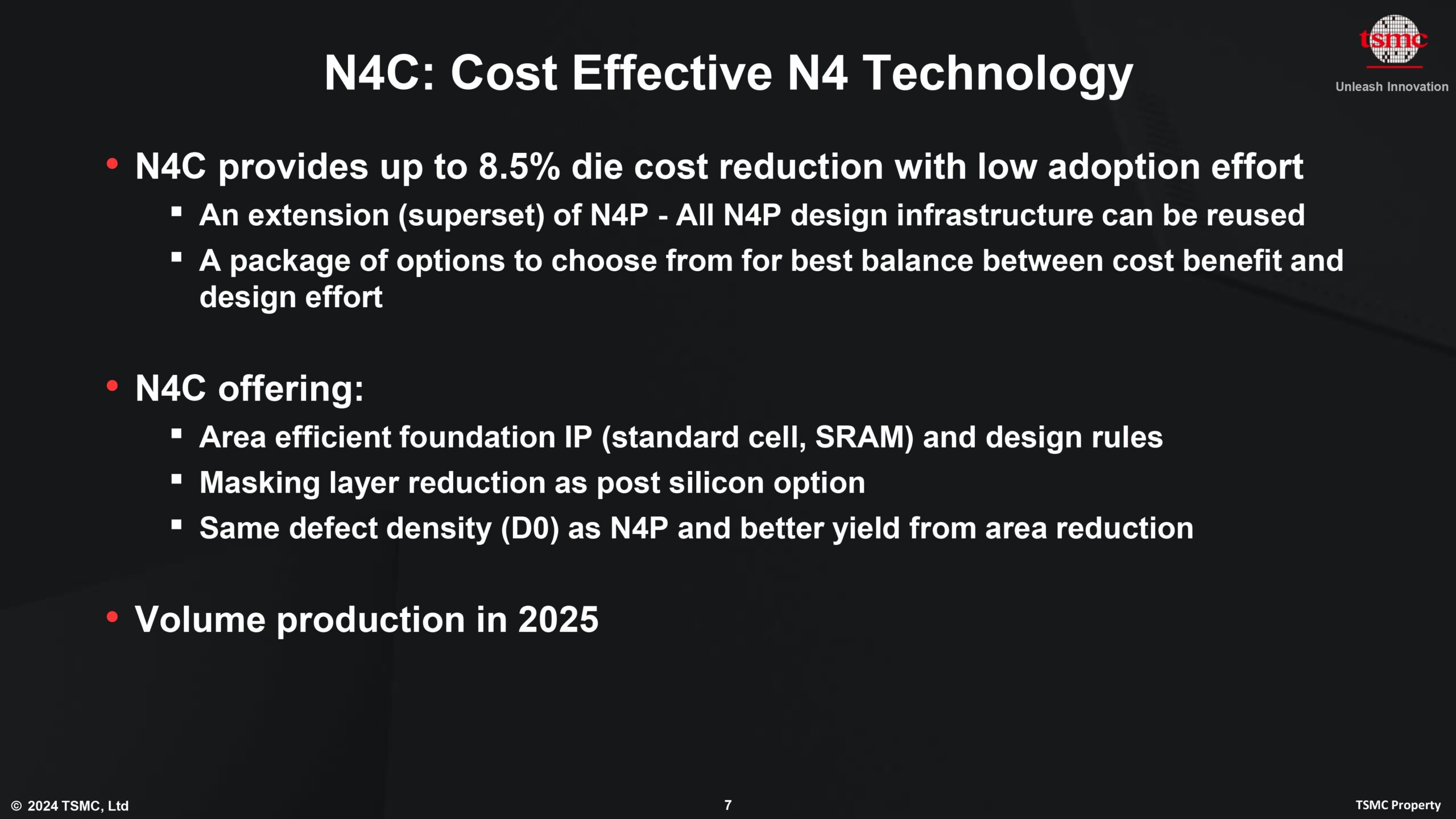
The Taiwanese firm also offers several options for chip firms to focus on cost or design efforts. While big-name brands like Apple, AMD, MediaTek, Nvidia, and Qualcomm aim to use TSMC’s 3nm process for their flagship chips, many chip firms will likely use the N4C process for their non-flagship chips to reduce fabrication costs and create value-for-money chips. Chips based on N4C could be released sometime next year, and the process could be used for years to come.

In comparison, Samsung has recently released the Exynos 2400 chip based on its third-generation 4nm process. Its fourth and fifth-generation 4nm processes are expected to be ready later this year and in 2025. However, the company hasn’t promised any figures for their efficiency and performance.

TSMC promises to start mass production of 1.6nm chips in 2026

TSMC 1.6nm 2nm 3nm Chip Fabrication Process Technology Roadmap 2024

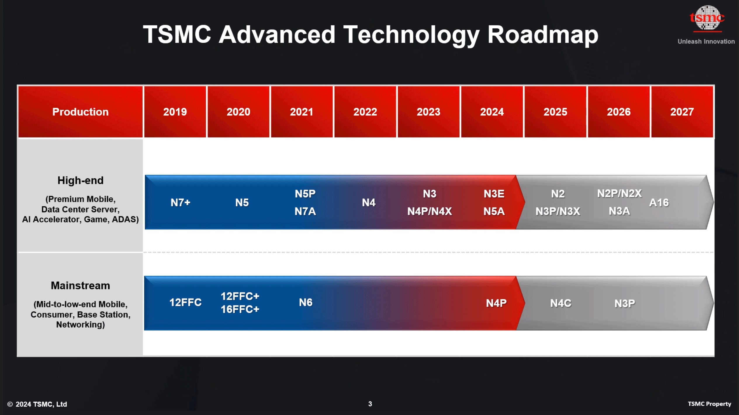
TSMC also unveiled its first Angstrom-class chip manufacturing process, A16 (1.6nm). It will be the first process to use Backside Power Delivery Network (BSPDN) technology for massive performance and power efficiency improvements. The BSPDN technology was promised to be used in TSMC’s 2nm process, but it has been removed from 2nm and will debut in 1.6nm chips.

A16 will also use Gate-All-Around Field-Effect Transistor (GAAFET) to increase transistor density. This technology has already been used in Samsung’s 3nm process, but we haven’t seen its results yet. No PC or smartphone chip made using Samsung Foundry’s 3nm process has been released yet.

TSMC is promising performance improvement of 8% to 10% at the same power and complexity as the N2P process. Chips using the A16 process can offer 15% to 20% improved power efficiency at the same frequency and transistor count. Regarding transistor density, TSMC claims A16 offers a 7% to 10% improvement.

[ad_2]

Source Article Link

Categories
News

Apple Partner TSMC Unveils Advanced 1.6nm Process for 2026 Chips

[ad_1]

Apple chipmaker TSMC has announced plans to produce highly advanced 1.6nm chips that could be destined for future generations of Apple silicon.

apple silicon 1 feature
TSMC yesterday unveiled a series of technologies, including the “A16” process, which is a 1.6nm node. The new technology significantly enhances chip logic density and performance, promising substantial improvements for high-performance computing (HPC) products and data centers.

Historically, Apple is among the first companies to adopt new, state-of-the-art chip fabrication technologies. For example, it was the first company to utilize TSMC’s 3nm node with the A17 Pro chip in the iPhone 15 Pro and ‌iPhone 15 Pro‌ Max, and Apple is likely to follow suit with the chipmaker’s upcoming nodes. Apple’s most advanced chip designs have historically appeared in the iPhone before making their way to the iPad and Mac lineups, and ultimately trickling down to the Apple Watch and Apple TV.

The A16 technology, which TSMC plans to begin producing in 2026, incorporates innovative nanosheet transistors along with a novel backside power rail solution. This development is expected to provide an 8-10% increase in speed and a 15-20% reduction in power consumption at the same speeds compared to TSMC’s N2P process, alongside up to a 1.10x chip density improvement.

TSMC also announced the rollout of its System-on-Wafer (SoW) technology, which integrates multiple dies on a single wafer to boost computing power while occupying less space—a development that could be transformative for Apple’s data center operations. TSMC’s first SoW offering, which is already in production, is based on Integrated Fan-Out (InFO) technology. A more advanced chip-on-wafer version leveraging CoWoS technology is slated for readiness in 2027.

TSMC is also making progress toward manufacturing 2nm and 1.4nm chips that are likely destined for future generations of Apple silicon. Its 2nm “N2” node is scheduled for trial production in the second half of 2024 and mass production in late 2025, to be followed by an enhanced “N2P” process in late 2026. Trial production of the 2nm node will begin in the second half of 2024, with small-scale production ramping up in the second quarter of 2025. In 2027, facilities in Taiwan will start to shift toward production of “A14” 1.4nm chips.

Apple’s upcoming A18 chips for the iPhone 16 lineup are expected to be based on N3E, while the “A19” for the 2025 ‌iPhone‌ models is expected to be Apple’s first 2nm chip. The subsequent year, Apple will likely move to an enhanced version of this 2nm node, followed by the newly announced 1.6nm process.

Each successive TSMC node surpasses its predecessor in terms of transistor density, performance, and efficiency. Late last year, it emerged that TSMC had already demonstrated prototype 2nm chips to Apple ahead of their expected introduction in 2025.

[ad_2]

Source Article Link